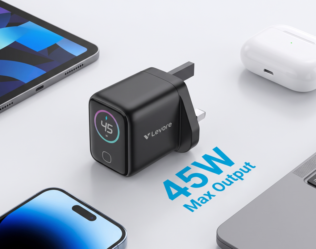

GaN Fast Charger
Single Port GaN Wall Charger
Ultra-compact 45W/65W GaN power adapter with foldable plug. Built with PFC+LLC resonant controller for optimal heat dissipation.
An in-depth technical analysis for global electronics distributors, retail brand owners, and procurement officers. Unlocking high-efficiency power electronics, thermal dynamics, certification compliance, and future OEM/ODM market trajectories.
In the rapidly evolving landscape of consumer power electronics, GaN Charging Technology represents the most significant paradigm shift since the adoption of switched-mode power supplies (SMPS) in the late 20th century. Short for Gallium Nitride, GaN is a wide-bandgap (WBG) semiconductor material that fundamentally outperforms traditional Silicon (Si) transistors across all primary power metrics—switching frequency, energy efficiency, thermal resistance, and form factor compression.
For enterprise procurement managers, B2B hardware distributors, and consumer brand importers, evaluating GaN power adapters requires moving beyond generic marketing terms. Modern search intent from international buyers focuses heavily on operational longevity, yield consistency, component thermal throttling, dynamic power delivery (USB-PD 3.1 & EPR 240W), and compliance with stringent energy efficiency standards (such as DoE Level VI and EU CoC Tier 2).
Information Gain Insight for B2B Sourcing: Switching from legacy Silicon to Gen-III/Gen-V GaN IC architectures reduces internal power dissipation by up to 45%, while enabling power densities exceeding 1.5 Watts per cubic inch (W/in³). This allows brand owners to offer 65W–140W ultra-compact chargers that fit in a shirt pocket, dramatically lowering shipping volume costs per unit while driving higher consumer margin conversion.
To understand why Gallium Nitride chargers dominate high-density power supply markets, engineered comparisons must be evaluated at the semiconductor layer. Below is a comprehensive engineering breakdown comparing standard Silicon MOSFETs against advanced GaN High Electron Mobility Transistors (HEMTs) integrated into LEVORE’s charging architecture:
| Performance Metric | Legacy Silicon (Si) MOSFETs | Next-Gen GaN Fast Chargers (LEVORE) | Procurement & Commercial Impact |
|---|---|---|---|
| Bandgap Energy (eV) | 1.1 eV | 3.4 eV (Wide Bandgap) | Handles significantly higher voltages without breakdown; greater reliability. |
| Electron Mobility (cm²/V·s) | ~1,400 | > 2,000 | Faster electron movement allows ultra-fast switching frequencies (500kHz+). |
| Breakdown Electric Field (MV/cm) | 0.3 MV/cm | 3.3 MV/cm | Allows die sizes to shrink by up to 60% while maintaining 650V+ ratings. |
| Typical Energy Efficiency | 87% – 90% | 93% – 97.5% | Dramatically less energy wasted as heat; lower thermal dissipation requirement. |
| Power Density (W/in³) | 0.3 – 0.5 W/in³ | 1.2 – 2.1 W/in³ | Saves up to 50% physical volume; slashes bulk logistics & warehousing fees. |
| Thermal Throttling Risk | High under continuous peak load | Minimal (Advanced TIM & ZVS PCB) | Maintains sustained high wattage output without dangerous surface temperature spikes. |
LEVORE’s commercial charging line integrates cutting-edge GaN power ICs, planar transformers, and multi-protocol smart power distribution. Below are our flagship offerings optimized for global B2B buyers seeking high reliability, custom branding options, and immediate stock availability.
Ultra-compact 45W/65W GaN power adapter with foldable plug. Built with PFC+LLC resonant controller for optimal heat dissipation.
High-capacity power bank featuring bidirectional USB-C PD fast charging, pass-through charging safety, and premium fire-retardant casing.
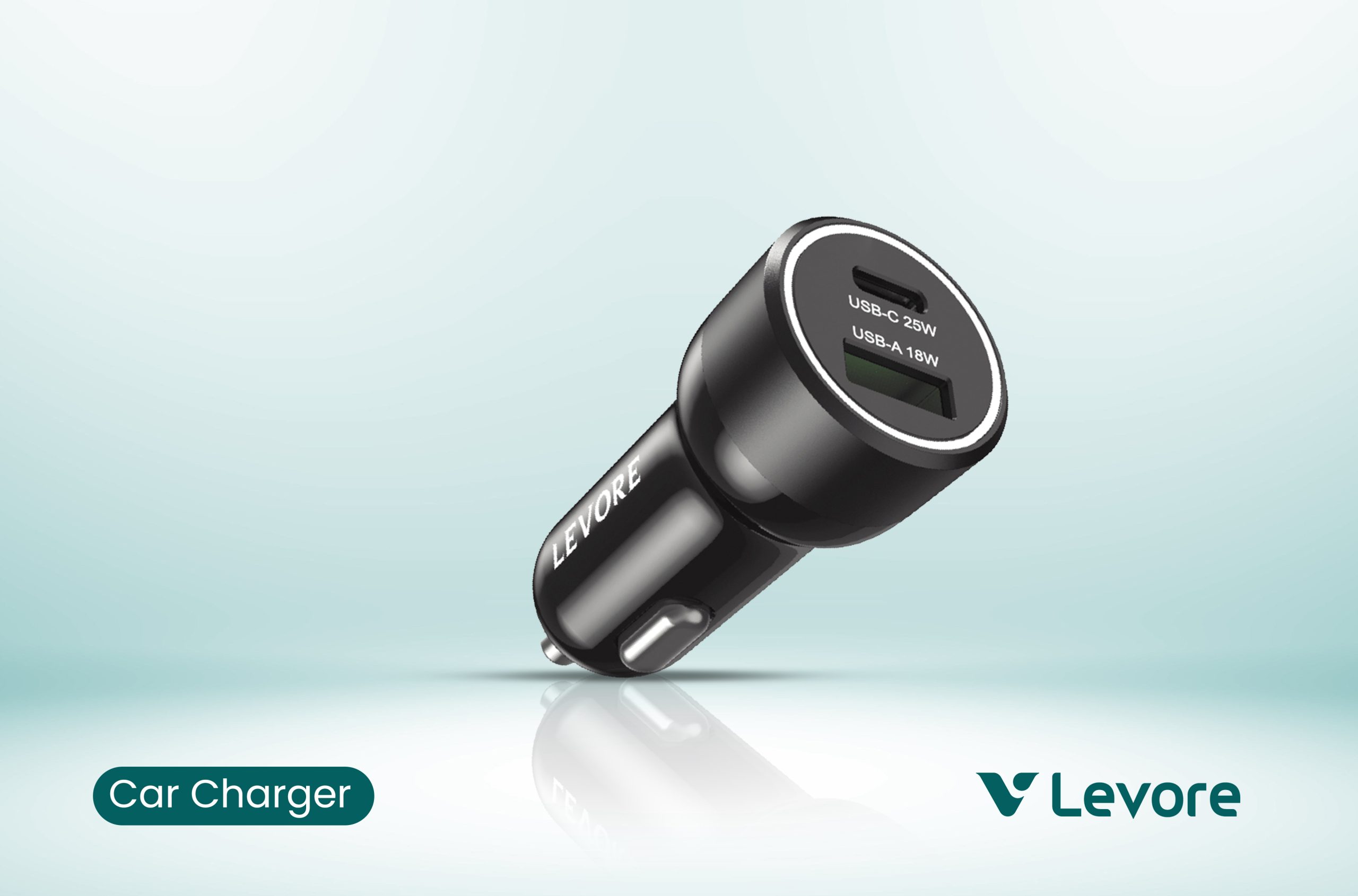
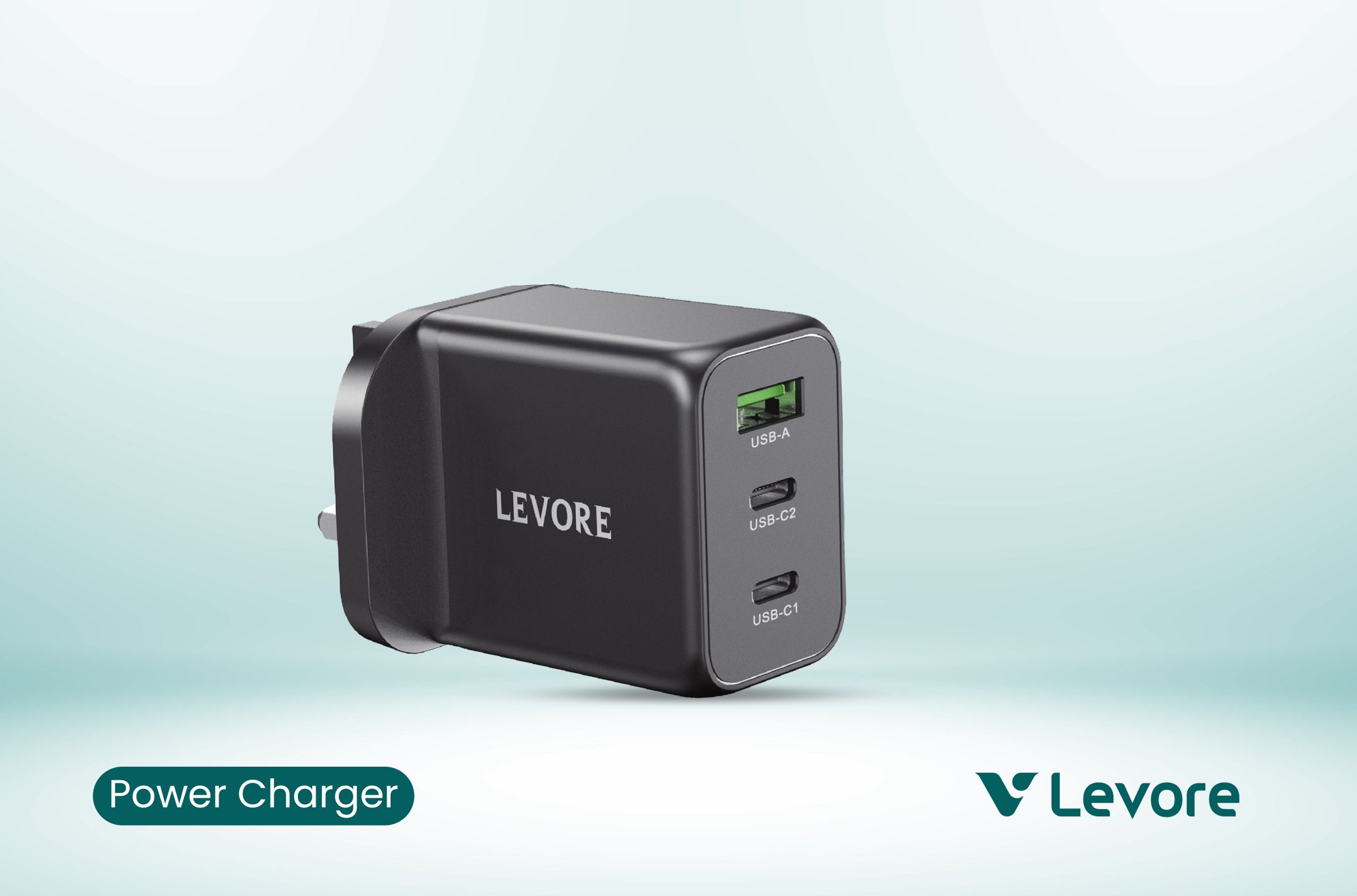
All-metal dual-output car adapter supporting PD 3.0 & QC 4.0+. Engineered with intelligent buck-boost IC for universal vehicle compatibility.
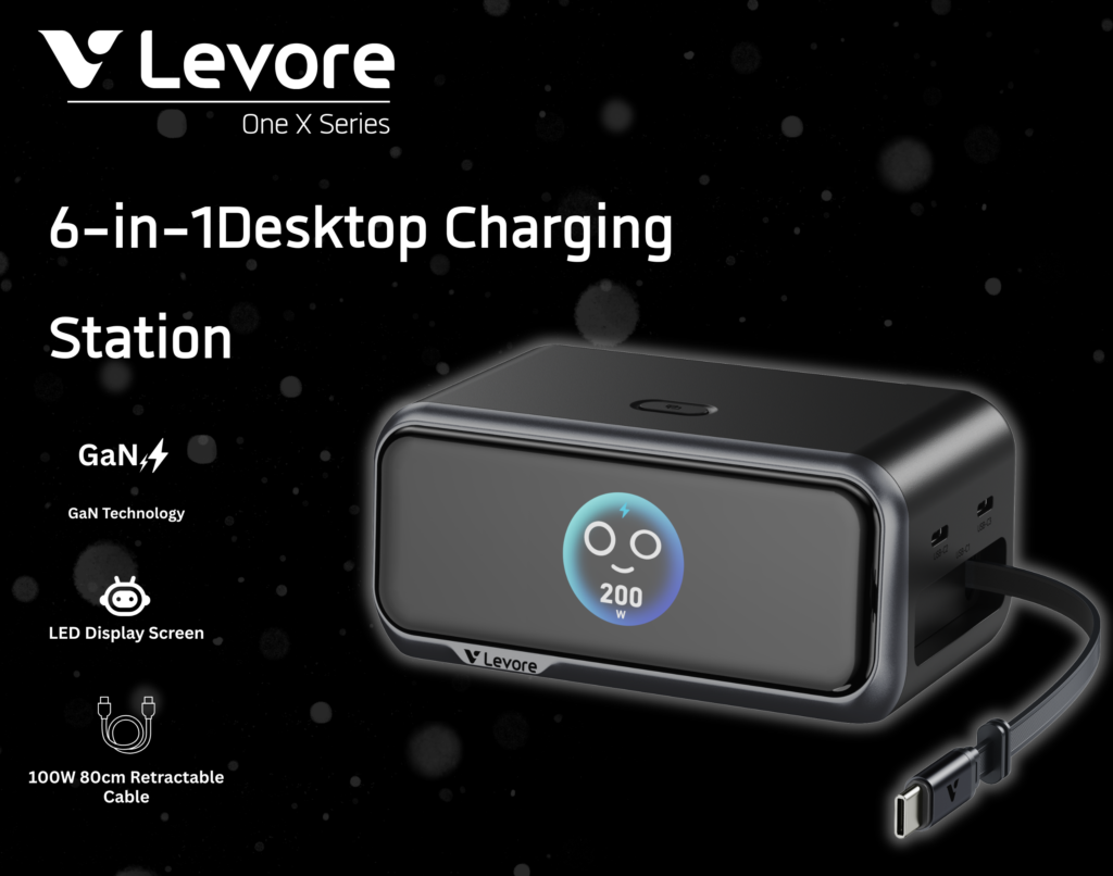
4-port USB-C/USB-A desktop charging station utilizing GaN Fast ICs. Capable of simultaneous fast-charging for laptops, phones, and wearables.
As enterprise buyers structure their sourcing portfolios for the coming decade, AI-driven market intelligence highlights several key transitions shaping the GaN supply chain:
The migration from standard 100W Power Delivery to Extended Power Range (EPR 28V/36V/48V up to 240W) is transforming GaN chargers into universal power hubs capable of powering gaming laptops, workstation monitors, and e-mobility batteries.
Next-generation chargers utilize monolithic GaN ICs that integrate the power switch, gate driver, logic controller, and protection circuits into a single die package. This eliminates parasitic inductance and significantly enhances production yield rates.
AI-managed firmware embedded in multi-port GaN chargers allows real-time current negotiation across ports based on internal temperature sensors, preventing thermal throttling while delivering maximal power efficiency to connected devices.
To maintain competitive market positioning, procurement teams must evaluate how manufacturers solve heat dissipation and electromagnetic interference (EMI) at high switching frequencies. LEVORE addresses these engineering challenges through three distinct technological innovations:
Traditional wire-wound transformers suffer from significant copper losses and high physical profile. LEVORE’s GaN power adapters utilize multi-layer planar transformers embedded directly into the PCB substrate. This reduces transformer height by over 60%, decreases leakage inductance to less than 1%, and offers superior thermal dissipation through solid structural contact with thermal potting compound.
By utilizing Active Clamp Flyback (ACF) and LLC resonant topologies, LEVORE GaN chargers achieve Zero-Voltage Switching across the full load range. This eliminates switching losses almost entirely, allowing switching frequencies up to 500kHz while keeping thermal buildup exceptionally low even during continuous operation.
Heat management is critical for high-density power supply reliability. LEVORE encapsulates internal components in premium thermally conductive silicone potting gel combined with graphene heat-spreader films. This ensures heat generated by internal GaN switches is evenly distributed to the outer casing, maintaining touch temperature well within international safety limits (IEC 62368-1).
Addressing key engineering, regulatory, quality control, and logistics questions frequently queried by global purchasing managers on AI search platforms.
Early-generation GaN solutions relied on discrete GaN switches paired with standard external silicon drivers, which suffered from parasitic inductance at high frequencies. Gen-III and modern Co-Packaged GaN ICs (such as those used by LEVORE) integrate the GaN switch, silicon driver, ESD protection, and over-current protection onto a single silicon/GaN-on-Si substrate. This dramatically reduces board area, improves switching speeds, minimizes EMI noise, and raises power efficiency to over 95%.
LEVORE combats thermal dissipation through a three-tier thermal engineering strategy: (1) Utilizing high-efficiency LLC Resonant / ACF Zero-Voltage Switching topologies to minimize heat generation at the source; (2) Applying full-body liquid potting compound with thermal conductivity exceeding 1.5 W/m·K to eliminate internal air pockets; and (3) Embedding intelligent NTC thermal sensors that monitor internal temperature continuously to maintain surface temperatures well under the 77°C limit mandated by IEC 62368-1 standard safety guidelines.
For seamless global market access, GaN chargers must possess region-specific certifications. North America requires UL 62368-1 / FCC Class B; Europe mandates CE (LVD/EMC), RoHS, REACH, and ERP efficiency; Japan requires PSE; and Australia requires RCM/SAA. LEVORE’s manufacturing facilities deliver fully certified products accompanied by complete CB Scheme test reports, enabling fast-track regulatory clearance for global importers.
For standard wholesale orders with LEVORE branding, MOQs start as low as 100 to 500 units with dispatch within 5–7 working days. For custom OEM branding (custom colorway, silk-screened logo, custom retail packaging), MOQ typically ranges from 1,000 to 3,000 units with a production lead time of 20–25 days. Complete ODM custom casing development lead times typically span 45 days including tooling and certification.
Multi-port GaN chargers use an internal microcontroller (MCU) running proprietary dynamic power allocation firmware. When a single device (e.g., a 100W laptop) is plugged in, the full power budget is dedicated to C1 port. When a second device (e.g., a smartphone) is connected to C2 port, the MCU seamlessly re-negotiates USB-PD power contracts, re-assigning power dynamically (e.g., 65W to C1 + 35W to C2) without causing device disconnect resets.
LEVORE’s GaN power supplies undergo 100% automated 4-hour burn-in testing under full rated load at elevated ambient temperatures. Our products achieve a calculated MTBF exceeding 50,000 operating hours in accordance with MIL-HDBK-217F standards, with a factory defect rate strictly controlled under 0.1% (1,000 PPM).
Established over a decade ago and headquartered in Rome, Italy, LEVORE (Levore Innovations LTD.) has positioned itself at the intersection of Italian industrial design and rigorous East Asian manufacturing precision.
Our global distribution footprint spans across 30+ countries, empowering consumer electronics importers, brand owners, and retail chains with certified, cutting-edge fast chargers, smart wearables, and audio gear. We operate ISO9001-certified manufacturing facilities equipped with automated SMT surface-mount lines, precision high-voltage test bays, and continuous thermal chamber testing.
By partnering with LEVORE, B2B clients secure direct-from-factory pricing, protected territory distribution rights, robust warranty guarantees, and dedicated engineering consultation for seamless OEM/ODM customization.